Xilinx FPGA with AVRILOS
Summary
In a previous article I presented the AVRILOS round-robin operating system. In this article I will describe the process to integrate FPGA configuration data into your code and be able to configure FPGA devices without the need of an external serial or PROM/Flash. This will reduce chip count if you integrate FPGAs with a microcontroller as I often do. Also I will present a simple VHDL SSI/SPI interface in VHDL that you can use as peripheral FPGA which you can control through AVRILOS. The example application is a 8 channel R/C Servo controller which is demonstrated through a video presentation.Relative Links
Introduction
There are two kinds of users that may need the information presented in this article.The first category consists of users that do not know how to design FPGAs or at least are not involved with this process. These users are interested to just download FPGA designs from third party bitstreams that need to incorporate to their embedded designs.
The second category are users that fully implement their designs which include FPGA devices. These users have or need full control of their flow and design parameters.
I assume that you have read the previous article on how to generate C source code from a bitstream FPGA file using my tool cvtfpga3.exe. If you haven't the link is here.
In this article you will see how to perform SRAM-based FPGA configuration through the SPI interface. Also you will see how to link and control your FPGA design with your microcontroller through a 3-wire interface.
I will use the open source AVRILOS operating system presented in this article. In the current article I will provide the AVRILOS extensions of configuring the FPGA and interfacing your design through the SSI interface.
The example application will be to demonstrate a multichannel RC servo peripheral controlled by the microcontroller using SSI (Synchronous Serial Interface. Ie. SPI). The code provided will be the next AVRILOS release which supports this functionality along with VHDL sources of the demonstrated design.
The VHDL SSI interface can be used to interface any logic you need and provides a standard microprocessor interface through which you can access your new blazing circuit.
Additionally I have made some improvements to the makefile scripts of AVRILOS.
Background
Microcontrollers are very popular because they can easily control systems and they are flexible. Nowadays microcontrollers have bigger memory capacities and a bunch of peripherals that can do almost everything.Another class of devices that have similarities with microcontrollers is the programmable logic devices called CPLD (Complex Programmable Logic Device) or FPGA (Field Programmable Gate Arrays).
As I design both FPGAs and microcontrollers my favorite setup is to make combo designs. I use a microcontroller for my main logic while I add up an FPGA for peripheral expansion. FPGAs offer logic gates, Flip-flops and many I/O which I can use to extend a conventional AVR DIP40 package. Because I have enough memory to the microcontroller I include the FPGA configuration inside the Flash eliminating this way the external serial PROM/Flash.
In this process presented here I assume that you know how to write, simulate, synthesize, place & route and generate the final bit-stream of the FPGA. Although I will present this technique for Xilinx Spartan devices, you can use virtually any device (and microcontroller of course).
Description
Aim of the project
Aim of the project is to have a platform for easily integrating FPGA and microcontrollers in a single design.Tools
The tools I use for AVRILOS are:- (SW) WinAVR (AVR GCC for windows).
- (SW) Atmel AVR Studio (for Simulation).
- (SW) Your preferable Editor.
- (SW) Terminal Program (ie. Terminal, PuTTY).
- (SW) Programmer software (AVRDude is already included in WinAVR but you might use AVREAL32 if you want).
- (HW) Hardware Board where you controller & FPGA lives!
- (HW) Programmer Dongle for AVR.
- (HW) USB/RS232-TTL Serial Level Converter for connecting to Monitor.
- Xilinx Spartan4K development tools
- (SW) CvtFPGA, tool to convert HEX or BIN files to C array code.
- GNUWIN32 (for makefiles if I don’t use the WinAVR ie. Other compiler packages like MPLAB)
- (HW) Oscilloscope (recommended)
- (HW) Multimeter (nothing less than that!)
- Anything else you can imagine and fits.
AVRILOS & FPGA
Directory Structure
The directory structure is as follows: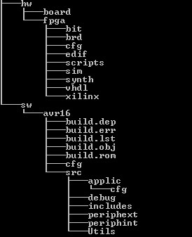
There are two major directories, HW and SW.
- HW is the directory where all my hardware development is done. This includes board schematic & PCB files as well as FPGA design.
- SW is the software tree of the microcontroller, more on this you can find in my first article for AVRILOS.
- Directory VHDL: Here are my source files for the FPGA.
- Directory CFG: Contains FPGA configuration files like constrain files where pin-locking and timing directives are placed.
- Directory Scripts: contains makefiles and other scripts.
- Directory SIM: Here I put the source files where I perform the simulation. Also any simulation scripts are placed here as well.
- Directory Synthesis: Here I put the files for doing the logic synthesis.
- Directory EDIF: The generated synthesis output is put here.
- Directory Xilinx: Place & Route, and general Xilinx flow.
- Directory BIT: The final bitstream is put here.
- Directory BRD: Contains the generated C output.
Description of AVRILOS FPGA architecture
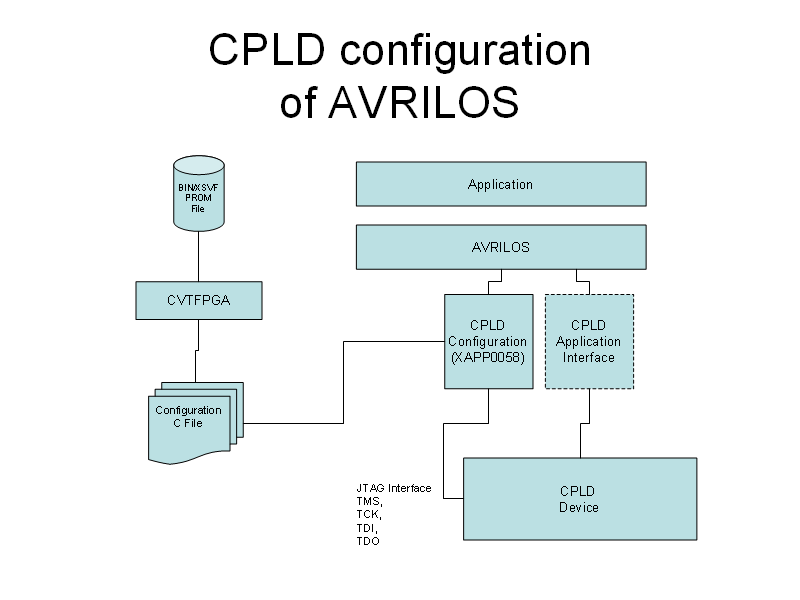
There are two major modules in AVRILOS regarding programmable logic.The first module is for the configuration or programming of the FPGA device. In case of CPLD the XSVF file will be executed only upon request to (re)program the CPLD after a logic change.
CPLD configuration of AVRILOS
The FPGA device however will need its code after each power-up.
FPGA configuration of AVRILOS
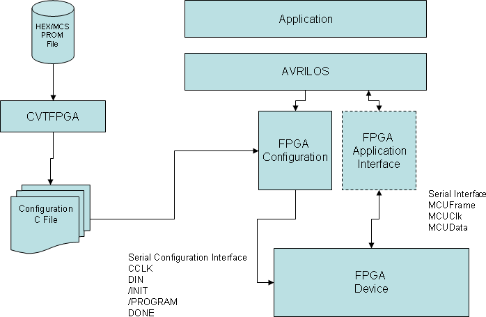
The second part is for the interface with the logic. This module is optional and is needed only if we need to control the programmable logic by the microcontroller. It could be possible that the FPGA can work independently from the microcontroller. For example such a case would be fixed counter, or an autonomous hardware controller. In this case this module is obsolete.
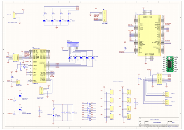
However if the FPGA need some control from the microcontroller you will need the corresponding module that interface to the specific FPGA. In each design you may have a different interface (both in hardware and in software that match), but this is not efficient if you want to re-use code. What I have concluded is to have an SPI/SSI interface which requires 3-4 I/O lines from the microcontroller and the FPGA and is a standard logic interface. This allows to have the basic FPGA communication routines same from project to project for the μC and same code for the FPGA. I just provide some constants in SW & HW that define how many registers we need to access in order to reduce gate-count in the FPGA side.See below for an example of interconnection between the CPU & FPGA. See below for the schematic.
Schematic (click for full-sized image)
Description of Modules (SW)
Module: xcs_cfg
I recommend reading the following PDF file from Xilinx:http://www.xilinx.com/support/documentation/application_notes/xapp098.pdf
This module has just one function:
void f_CfgSPIFPGA(void)This function is called during AVRILOS initialization before the main loop starts. As this process may take some time (hundred’s of milliseconds) it is better placed in the initialization area. Also any subsequent initializations of the logic (through the application interface) can take effect after configuration finishes.
I had an older version when I was configuring the old XC3000 series FPGA where the configuration was downloaded by bit-banging. This would allow better flexibility of pin assignment. However this method is slower than the SPI interface which is used by the current module.
You need the following FPGA I/Os to configure the in Slave-Serial mode:
PROGRAM (MCU Output), (b_Prog)
INIT (MCU Input during configuration), (b_Init)
DONE (MCU Input), optional, not used in this module
DIN (MCU Output), connect to SPI-MOSI, (b_Din)
CCLK (MCU Output), Connect to SPI-SCLK, (b_CClk)
This module requires that you have entered the correct pin assignments in the global settings file "include/settings.h" file:/**************** FPGA Configuration I/O ***********/
#define c_CFGPIN PINB
#define c_CFGPORT PORTB
#define c_CFGDDR DDRB
/* for Spartan/XL, XC4000 */
#define b_Init 3
#define b_Prog 2
/* Used with SPI */
#define b_Din 5 /* MOSI for SPI */
#define b_CClk 7
/* old definitions for XC3000 */
#define b_Reset b_Prog
#define b_Done b_InitIn the example above I am using only PORT-B for controlling FPGA configuration. SPI is at the same port and this simplifies initialization. Name convention is as follows:c_CFGPIN : Pin port, for direct Input capture c_CFGPORT: Port register for setting/reseting bits c_CFGDDR: Data direction RegisterThe bit-names
b_Done/b_Init, b_Reset, b_Din, b_CClk are associated with the corresponding bit position in port B. ie. B_Done/b_Init is assigned to 1, which means Port B, bit 1: PB1.The beginning of the file "periphext/xcs_cfg.c" contains I/O macros for direction and bit control of the I/Os. Thus we have an easy way to redefine I/O for each project through the "include/settings.h" file and keep our code easily readable. Direction settings as well as pin control are available as simple human-readable format commands.
Fragment of "periphext/xcs_cfg.c"
#define ToggleCCLK do{ \
                    cbi(c_CFGPORT, b_CClk); \
                    sbi(c_CFGPORT, b_CClk);    \
                    }while(0)
// Spartan Config SPI
#define    SetInit        do{ sbi(c_CFGPORT, b_Init);}while(0)
#define    ClrInit        do{ cbi(c_CFGPORT, b_Init);}while(0)
#define    InitInput      do{ cbi(c_CFGDDR, b_Init)  ;}while(0)
#define    InitOutput     do{ sbi(c_CFGDDR, b_Init)  ;}while(0)
#define    ClrCCLK        do{ cbi(c_CFGPORT, b_CClk) ;}while(0)
#define    ClrDin         do{ cbi(c_CFGPORT, b_Din)  ;}while(0)

#define    SetProg        do{ sbi(c_CFGPORT, b_Prog);}while(0)
#define    ClrProg        do{ cbi(c_CFGPORT, b_Prog);}while(0)
#define    ProgInput      do{ cbi(c_CFGDDR, b_Prog)  ;}while(0)
#define    ProgOutput     do{ sbi(c_CFGDDR, b_Prog)  ;}while(0)
…
The actual FPGA data that is downloaded must reside at the "applic/cfg/fpga_cfg.c/h" file. This is a copy of the "hw/fpga/brd" directory, generated by the cvtfpga3.exe tool.You might need to modify slightly the definition of the original generated
lut_cfgfpga[] constant for specific compiler directives as per below (for AVRGCC). INT8U __attribute__ ((progmem)) lut_cfgfpga[]={
0xFF, 0x04,
0xB0, 0xB4,
0xF9, 0xEA,
... If you use the makefile presented in the FPGA flow article you just need to copy and rename the file appropriately. If you have converted the bitstream with the -o AVRILOS option (make AVR) the file is compliant with AVRILOS. No internal modifications are needed.The first segment of the configuration function initializes the port direction. Then the configuration cycle is initialized and afterwards the data are downloaded. At the final stage success or failure is notified in
v_sysstat register.You can enable some debug information to be output to the serial port by enabling the corresponding macro:
#define DBGFPGA Then the status of Init signal will be reported at various stages.Initially the code asserts the
b_Prog bit in order to initiate a configuration cycle to the FPGA. Then waits until the b_Init input becomes high, meaning that the FPGA have cleared its configuration memory. During configuration data are downloaded in a synchronous manner. If there is an error in the process the b_Init will go low indicating an error. If downloading was successful the b_Init will remain high. This is an indirect way to determine that the FPGA is configured. Alternatively you must use one more pin and sample the DONE signal (active low). There are three possible actions you can take if configuration fails. You can either, retry, ignore and freeze.
Retry means that you can try to reconfigure the FPGA one or more times until success. However you should not have configuration errors unless you have a hardware issue. Also a retry mechanism will be more complex. And you could still not have a success.
Ignore means that you continue program execution, the FPGA success flag is not set and the microcontroller enters its main loop. You may notify the user, with a LED Alive different time value and do a graceful degradation if possible. This is demonstrated in the "applic/kernel.c" file:
#ifdef MOD_FPGAXCS_ON
    v_retval = f_CfgSPIFPGA();
    if (v_retval == c_FPGACFG_ERR) f_SystickSetErrLevel(c_ALIVEFPGAERR_ms);
#endif
If there is an FPGA configuration error the LED flashes with a different time period.Freeze means that program execution is halted on a infinite loop. Thus the microprocessor will not be operational and it might be immediately noticed by the user. Although this is a hard-core approach it might not be possible to do anything more useful.
At this piece of code I choose the Ignore option. It is the simplest approach and allows a graceful degradation if needed. Also the user is notified in case of error with a different LED flash period.
Module: FPGA SSI module
This module provides the communication layer that links the microcontroller with your hardware design. This file is linked with the SSI interface from the FPGA hardware. The interface is a simple SPI interface (3-wire) where we have multiplexed the input and output signals in one line (see relative diagram at the description). There are three main functions.f_InitSSI: Is called to initialize the module and do I/O direction.
f_FPGARd: Is used to read an FPGA register.
f_FPGAWr: Is used to write an FPGA register.
The Chip Select Signal is activated. Then 8-bits are transferred serially to the FPGA. The MSB contains the Read or Write bit information. This controls if the second byte to transfer will be an input or output (read or write operation). The rest of the bits are the register address to access. Then the second byte transferred is either data to program in this register (write) or the contains of the register (read). Data direction of the MCUData pin is controlled by the read/write bit for the second byte transferred.
The port definition of the SSI interface is defined at the "include/settings.h" file as per below:
/**************** FPGA Application I/O *************/

#define    c_IFCPIN        PIND
#define    c_IFCPORT        PORTD
#define    c_IFCDDR        DDRD

#define    b_MCUClk        7
#define    b_MCUFrame            6
#define    b_MCUData        3
We assume that all port bits controlling the SSI should be on the same port. In this case its the D port. An alternate way to do it is by using the SPI interface (you may wire the internal input-output data signals directly to MISO-MOSI without multiplexing them, resulting in a normal SPI 4-wire interface). This could be faster for transferring data to /from the FPGA but it may induce problems when you will try to reprogram the AVR through the SPI, because the FPGA interferes with the SPI. In such a case where I was using some of the SPI lines to do the SSI, I had to keep the FPGA reset in order to be able to reprogram the AVR.
Module: Debugger
I had provided debugger command extensions that control the main functionality of the FPGA access mechanism. The FPGA Read or Write operations.This functionality is summarized below:
Command & Format Summary
| Command | Description |
F 00XX | ReadFPGA reg XX (Custom Commands, depend on FPGA Code) |
f 00XX YY | Write FPGA Byte YY at reg XX (Custom Commands, depend on FPGA Code) |
U | Perform an FPGA reconfiguration, Custom Command |
Also I have modified the user debug command (
U) to manually reconfigure the FPGA for testing purposes. Normally I have a LED connected to the DONE output of the FPGA that is lit during configuration or in case of an unconfigured device. If the programming is successful then the LED shuts off, indicating (visually) that the logic is running. So in case I execute the "U" command the LED will activate for a few seconds and then it will shut off. IF something is wrong the LED will remain active indicating an error condition. Normally this should have to do with your interconnection hardware.These extensions are implemented in the file dbgext.c. You can provide you own commands on dbgext.c, but you need to modify the base debugger.c file as well to get the input and process the new commands. If you disable the FPGA SSI interface from your "scripts/hw.in" file then automatically this functionality will be removed. The functionality of the extra commands exists always in the debugger.c which calls the dbgext.c functions.
Keep in mind that robolayer.c updates FPGA PWM registers on evry loop run and this means that whatever you write at these registers you will not see anything because the value will be overridden almost immediately. However the frequency and LED registers can be tested (these are not updated).
Module: Serial Application
Please refer to the first article of AVRILOS for detailed explaination of the serial application.In this example I have programmed the following commands:
Motor H-Bridge Driver
q: Increase Motor Power (Rear wheels)a: Decrease Motor Power (Rear wheels)RC Servo
o: Turn front wheels left.p: Turn front wheels right. l/k: Close/Open gripm/n: Turn head right/left Module: Motor
This module is a copy paste of the Timer1.c. However there are changes to support an H-Bridge dual driver. This configures the PWM frequencies for motor (in contrast Timer1.c used low frequency signals for servo control). Also provide functions to allow brake, stop, forward or backward motion. It is has a very simple interface where you can select the channel on which you want to function.Description of Modules (HW)
Module: SSI Interface
I will describe the SSI interface logic from the FPGA side. The SSI block consists from SSISync, SSIBitCnt, SSIFSM, SSIDecoder, SSIShifter & SSIRego.SSI Interface
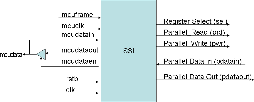
SSISync does the input synchronization. As we have a high frequency system clock, all signals are synchronized with this clock (even MCUClk, the software clock to shift data to the FPGA). So this block introduce the interface signals to the internal logic, avoiding metastability issues.SSIShifter shifts serially the data and presents a parallel output representation, beeing effectively a SIPO register (Serial-In, Parallel Output). Also the MSB of this register is the serial output of the logic thus performing a PISO (Parallel-In, Serial Output).SSIBitCnt implement a counter that increment on each bit clock. This counter is used by the FSM to provide control to the system for reading or writing registers.SSIFSM provide all the control signals to shift, load, read or write the registers. It is the main control unit for the communication.SSIDecoder enables the corresponding register to link with the SSI interface. Each operation (read/write) is performed on the selected register.SSIRego is a register class that implements the register output of the SSI interface. This is the final data destination of each communication. Also in read mode its parallel output is loaded to the shift register in order to shift serially the data out. The timing details are shown below. Data are always transmitted from MSB to LSB. First phase is the Address phase, where the R/W bit is the MSB (0: Write, 1: Read), then comes the 7-bit of the address. If you need less registers the unused MSB address bits are don't cares, but my norm is to write don't cares as zeros. Second phase is the Data Phase. If MCU writes the FPGA the MCUData I/O does not change direction and we write the register. If direction is to read then MCUData becomes an output in the FPGA (and AVR should change direction as well in order to not induce a signal conflict). The coomunication clock due to sampling limitations should have frequency below master clock divided by 4. ie. 8MHz clk in this case, provides a maximum MCUClk of 2MHz.
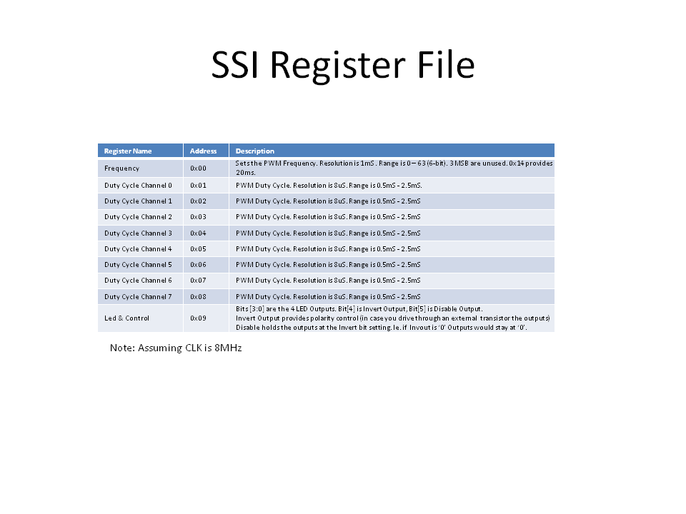
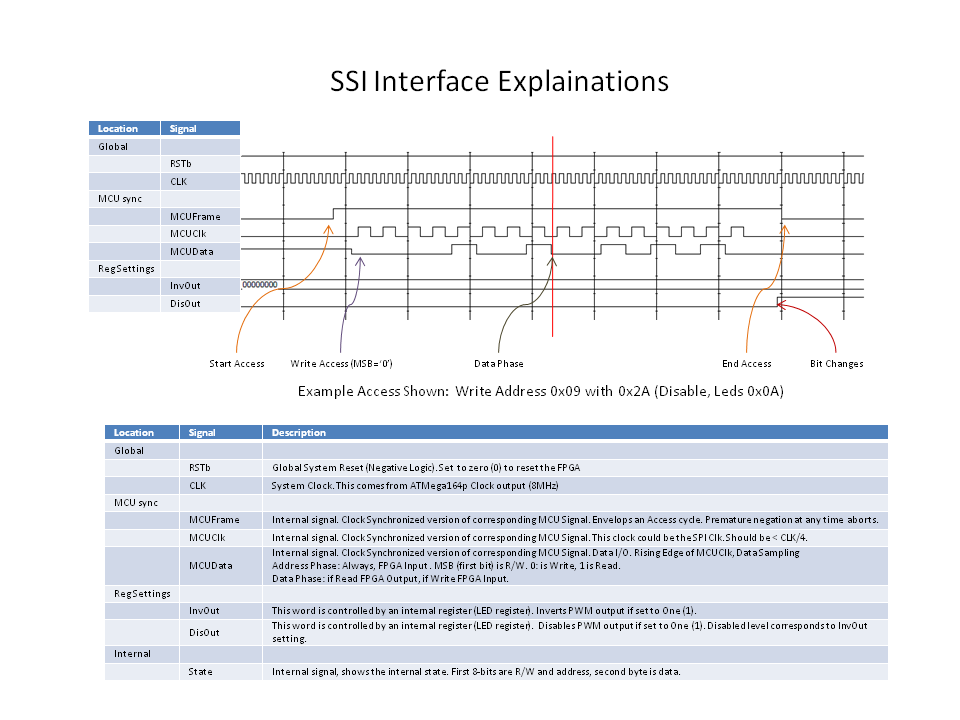 Because reading back registers consumes resources i made only two registers readable (Frequency and LED). All other registers are Write Only. If you try to read them you will get 0xFF.
See below for the register file used.
Module: PWM
Although this module is named pwm it implements an 8-channel R/C Servo controller. Actually the number of channels are programmable by changing the avrilos_pkg.vhd file:PACKAGE avrilos_pkg IS
CONSTANT cMaxChan: integer := 8;
CONSTANT cMaxAddr: integer := 4;
CONSTANT cMaxRegs: integer := 10;
CONSTANT cADDR_FQBASE: integer := 0;
CONSTANT cADDR_PWMBASE: integer := 1;
CONSTANT cADDR_LDBASE: integer := 9; The constant cMaxChan can be changed in order to increase or decrease the number of channels. You may need to adjust cMaxAddr and cMaxRegs to match the maximum address bits required as well as maximum number of registers to access.
The architecture is shown below:
PWM Servo Control
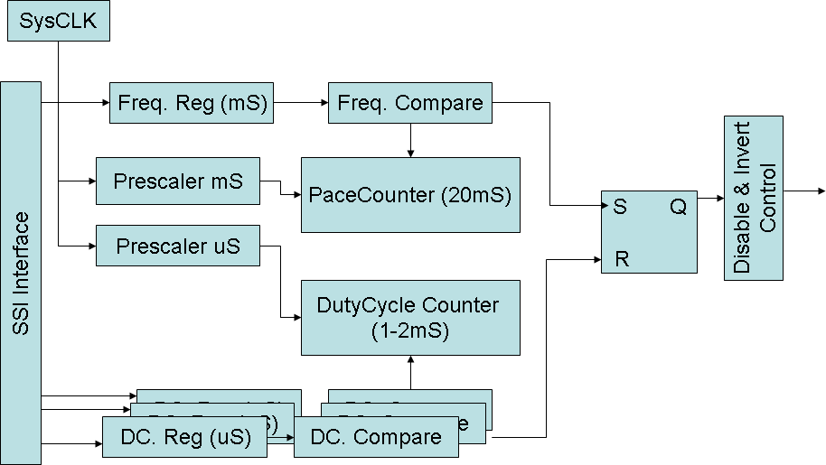
The idea is simple. There is the master clock (in this case 8MHz). This clock is divided in order to produce two timebases:
- 0.5ms frequency control (start of pulse).
- 8μs step that controls the width of the pulse.
This frequency is common to all channels.
Each channel has a programmable pulse width. The minimum width is 0.5ms (0x00) and the maximum width is 2.5ms (0xFF). The mid position is at 1.5ms (0x7F). Although the nominal values should be between 1-2m, there are some times servos that have a different range. So for these cases I have provided a wider range that allows various subsets of periods to be used, depending your hardware.
Due to FPGA size restrictions only the frequency and LED registers can be read-back by the SSI. For testing purposes this is enough. If there is a problem you can verify that a write access to the frequency register has performed well or the read-back value is irrelevant to the written value, providing a hint that something is wrong.
Also from the LED register there are two control bits available. One (bit 5) for disabling output (no pulses are generated), and the second (bit 4) to invert the output So one have full control of the generated waveform. Keep in mind that if the output signal is inverted and you disable the output, the default state will be '1' instead of '0'.
System setup
This release of AVRILOS has some more enhancements for easier environment adaptation. The file "cfg/env.in" contains two new variables:PROGPORT = COM3
PROGDEV = avrispv2 These two variables define the output COM port for avrdude and the programmer type. Thus if you use a different hardware than mine you will need to change only the environment configuration file.In the file "cfg/hw.in" you define if you need to perform FPGA configuration and you need to include the SSI interface:
# select FPGA Configuration
# FPGA Configuration from AVR
# 2: AVR Configures FPGA XCS Spartan
# 1: AVR Configures FPGA XC3K (legacy)
# 0: FPGA configures itself from PROM
    ADD_FPGA_CFG    = 2

# FPGA SSI Interface (FPGA slave)
    ADD_FPGA_SSI     = 1
For ADD_FPGA_CFG the valid values are 0 (disable) or 2 (enable). The option 1 (enable XC3K) is not supported. I used this when I had to support both XC3K and Spartan devices.The
ADD_FPGA_SSI is needed only when you need to control your logic from the microcontroller. You do not need this if you implement a different communication interface or if your logic is independent from the controller.The file "cfg/swdef.in" has added fuses control for individual microprocessors.
For example the ATMega164p I am using in this example does a clock output (crystal frequency 8MHz) at Port.B1. I have also disabled the JTAG interface because I am not sing a JTAG programmer for this part and I need the JTAG ports for normal I/O. There are sites that compute the fuses for you like the following: http://www.engbedded.com/fusecalc/
Put your parameters and compute the fuses. Then put your l/h/efuse parameters at the corresponding controller section like this:
ifeq ($(MCU),atmega164p)
    CDEFS := $(CDEFS) -Dc_MCU=3
    PMCU = MEGA164P
    PMCU2 = m164p
    lfuse = 0xa7
    hfuse = 0xd9
    efuse = 0xff
endif
Cfg/Srcobj.in file is updated with the new sources to support the extra FPGA functionality.Example Usage
Our example Application will implement the basic functions to support a small robot. What i will present is one hand-made board that controls a motor for motion, a servo for direction control, another servo for head direction (which incorporates an IR distance sensor), and a servo grip. The block diagram of the board is shown below:Hardware Block Diagram
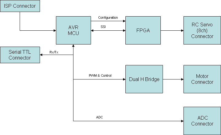
See detail schematic in the beginning of the article.
In this example i have provided an intermediate robolayer.c which provides a higher level of control. This layer provide an easy interface for a higher layer which will control the robot. I have not build that yet, but the code provided is adequate to demonstrate the capabilities of FPGA integration with a microcontroller. Please see the relevant video.
AVRILOS & FPGA Video
There are two major sections in this video. The first has the application running at specific intervals (defined at ifc_time.h, c_AppInterval_ms). Because many keys are accepted before the next application iteration motion is not smooth. When i move the application to run at every main loop (or i could increase the Application frequency) the motion gets smoother.
Conclusion
In this article I presented an addition to the previous simple framework for including FPGA configuration and control, from your microcontroller design. I tried to do a streamline approach that will allow easier integration of different hardware with common communication functions. All these additional functionality is put within the AVRILOS framework. The advantage is that even users that do not have knowledge of the FPGA development, are able to use ready made FPGA designs done by other people to their own boards. The only restriction is the pin-locking. In case they have a proven design and it's synthesized netlist, they can run the rest of the FPGA flow (see previous related article) with specific pin-locking constrains, running a single script that generates the C source file needed by the current article.License
This article, along with any associated source code and files, is licensed under CDDL(http://www.opensource.org/licenses/cddl1.php)For any questions: avrilos[at]ilialex.gr
History
- Version 1.0, Initial Release.
- Version 1.1, Added more Hardware Detail of SSI.


I read your programming tips, it exactly that I need, but I prefer to use another easiest method with help of this innovative JTAG box https://gsmserver.com/item/boxes-and-dongles/z3x-easy-jtag-with-cables-and-jtag-isp-adapter-5-in-1/ cuz its very valuable device which may help u to save a lot of time and nerves! I have been using it for 2 months and that JTAG box actually amazing.
ReplyDelete